
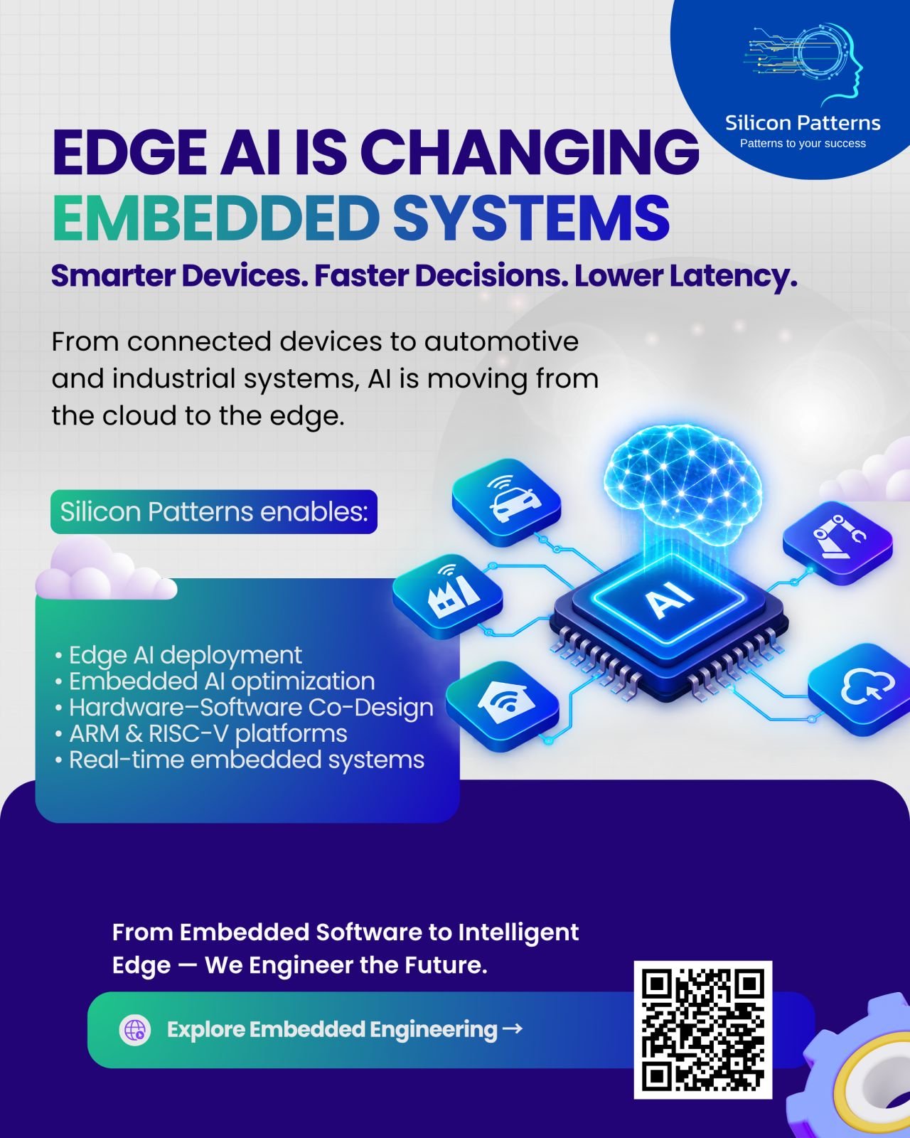
Silicon Patterns Semiconductor Design Services Madhapur Hyderabad
Comprehensive Semiconductor Design Services: From Architecture to GDSII Sign-Off
In the rapidly evolving world of technology, standard off-the-shelf microprocessors often fall short of meeting the specialized performance, power, and area (PPA) requirements of next-generation applications. From artificial intelligence and high-performance computing to automotive systems and smart IoT devices, custom silicon has become the ultimate differentiator for market leaders. Silicon Patterns provides elite, full-stack semiconductor design services, helping fabless companies, Integrated Device Manufacturers (IDMs), and high-growth startups transform complex ideas into production-ready silicon. With an exceptional 98% first-pass tape-out rate, our team of over 200 expert VLSI engineers ensures your ASIC or SoC design achieves zero-compromise quality, faster time-to-market, and optimized performance.
The Strategic Importance of Custom Silicon Design
Developing a custom Application-Specific Integrated Circuit (ASIC) or System-on-Chip (SoC) is a high-stakes endeavor. A single engineering oversight can lead to expensive silicon re-spins, missed launch windows, and blown budgets. Silicon Patterns mitigates these risks by combining industry-proven methodologies with full-flow expertise. Whether your goal is to minimize power consumption for a battery-operated wearable device, maximize throughput for an AI neural processing unit (NPU), or guarantee functional safety for an automotive ADAS chip, our engineering pods handle every layer of the silicon lifecycle with meticulous care.
Full-Stack Semiconductor Design Offerings
We offer comprehensive, end-to-end capabilities across the entire digital design flow. Our engineering team can take complete ownership of your turnkey ASIC project or integrate seamlessly as a dedicated pod within your existing structure.
1. Architecture & Microarchitecture Definition
Every successful chip begins with a solid structural blueprint. We bridge the gap between product requirements and physical reality during the foundational planning phase.
- System-Level Partitioning: Defining the core blocks, hardware-software boundaries, and bus fabrics to optimize data throughput.
- Pipeline Design: Creating efficient execution pipelines that balance clock frequency targets with computational latency.
- Power and Clock Domain Planning: Designing robust power management schemes, including dynamic voltage and frequency scaling (DVFS) and extensive clock gating.
- Performance Modeling: Executing cycle-accurate simulations and SystemC modeling to validate hardware architecture before writing a single line of RTL code.
2. High-Quality RTL Design & Coding
Our hardware description language specialists author clean, highly maintainable, and synthesizable code that serves as the bedrock of your physical hardware.
- Multi-Language Expertise: Writing production-grade RTL code using industry-standard hardware description languages including Verilog, VHDL, and SystemVerilog.
- Strict Coding Standards: Applying rigorous design rules to eliminate downstream synthesis bottlenecks and prevent logical vulnerabilities.
- Lint-Clean Delivery: Employing advanced static analysis and automated lint checks early in the development loop to catch design bugs before simulation.
3. Advanced Functional Verification
Functional bugs discovered after tape-out are catastrophic. We utilize state-of-the-art verification environments to guarantee your design meets its specifications under all real-world conditions.
- UVM Environments: Building robust, scalable, and reusable Universal Verification Methodology (UVM) constrained-random testbenches.
- Assertion-Based Verification (ABV): Embedding formal properties and assertions directly into the design to monitor internal signals dynamically.
- Formal Property Checking: Utilizing mathematical formal verification tools to exhaustively prove the correctness of complex control logic and protocols.
- Coverage Closure: Tracking statement, branch, and functional coverage systematically to achieve 100% verification confidence.
4. Design for Test (DFT) Engineering
A chip must not only work in theory; it must be fully testable on the manufacturing floor. Our DFT engineering practices guarantee excellent production test coverage while keeping silicon area overhead to a strict minimum.
- Scan Insertion: Setting up optimal scan chains and test compression mechanisms to accelerate manufacturing tests.
- Automatic Test Pattern Generation (ATPG): Creating high-fault-coverage test patterns to catch physical defects during high-volume manufacturing.
- Memory Built-In Self-Test (MBIST): Integrating automated self-test and repair logic for complex embedded memory arrays.
- Boundary Scan & JTAG: Designing standards-compliant test access ports for board-level testing and system debugging.
5. Physical Design & RTL-to-GDSII Sign-Off
We transform your logical RTL description into an optimized physical layout, solving complex physical challenges at advanced process nodes.
- Floorplanning & Placement: Conducting macro placement, power grid design, and standard cell placement to optimize utilization and routability.
- Clock Tree Synthesis (CTS): Constructing low-skew, balanced clock trees to minimize clock jitter and power dissipation.
- Static Timing Analysis (STA): Performing multi-corner, multi-mode static timing analysis to eliminate setup and hold violations.
- Physical Verification: Running exhaustive Design Rule Checking (DRC) and Layout Versus Schematic (LVS) validations to guarantee a completely clean GDSII file for foundry handoff.
6. Pre & Post-Silicon Validation
Our commitment to your project does not end when the files are sent to the foundry. We support your engineering lifecycle through hardware emulation and physical bring-up.
- Hardware Emulation: Accelerating pre-silicon software development and system-level validation using enterprise-grade hardware emulation platforms like Veloce and Palladium.
- Silicon Bring-Up: Writing robust bring-up scripts, configuring lab test gear, and performing initial hardware power-up sequences.
- Characterization & Debug: Investigating anomalies on physical silicon, validating real-world power profiles, and confirming production readiness.
Flexible Engagement Models & Node Support
We understand that every company faces unique resource constraints, budgets, and timelines. Therefore, we offer three highly adaptable engagement models:
- Full Project Ownership: Our engineering team takes end-to-end responsibility for the entire flow, managing your project from architectural specification to clean GDSII handoff.
- Dedicated Engineering Pod: A cohesive, multi-disciplinary team of VLSI specialists is assigned exclusively to your business, functioning as a seamless extension of your in-house engineering group.
- Staff Augmentation: Highly specialized senior engineers integrate into your existing structure to help you clear immediate bottlenecks, handle peak workloads, or fill highly niche technical gaps.
Our engineers possess extensive experience across a broad spectrum of fabrication processes. We support geometry sizes ranging from legacy 180nm, 130nm, and 65nm nodes for analog and mixed-signal applications, down to advanced FinFET and FD-SOI nodes like 28nm, 22nm, 16/12nm, 7nm, and 5nm technology nodes for high-performance compute chips. Being entirely tool-agnostic, our workflows integrate flawlessly with major electronic design automation (EDA) software from vendors like Synopsys, Cadence, and Siemens EDA.
Our Step-by-Step Spec to Silicon Process
Silicon Patterns utilizes an engineering-driven, transparent execution model that breaks down complex design lifecycles into predictable milestones:
- Step 01: Discovery & Specification Review: We conduct deep-dive technical reviews of your functional targets, target process nodes, performance objectives, and delivery schedules to catch architecture risks early.
- Step 02: Architecture & Planning: Our team writes comprehensive microarchitectural descriptions, partitions logic blocks, defines hardware interfaces, and builds cycle-accurate performance models.
- Step 03: Design & Verification: Engineers write clean RTL, while our verification team deploys UVM environments, running automated regressions with clear, weekly dashboard reporting.
- Step 04: Sign-Off & Tape-Out: We finish physical layout design, resolve timing bottlenecks, run final DRC/LVS physical sign-off checks, deliver the verified GDSII data to the foundry, and provide comprehensive post-silicon validation support.
Contact Address: 1st floor, #212, Silicon Patterns, KTC Illumination, Plot # 32 to 34 & 39 to 41, Vittal Rao Nagar, Madhapur, Hyderabad – 500081
Details
| Category | Computers and Web Services |
|---|---|
| Location | Hyderabad, Telangana |
| Posted On | Sep 23, 2026 |
When you call, don't forget to mention that you found this ad on PostFreeAds.
Share this ad
Recent Ads
-
 Car Detailing Services in Vijayawada, Hyderabad, Rajahmundry, Visakhapatnam | DetailR
-
 Digital Marketing, Web & IT Solutions for Business Growth | WebMeHigh Ahmedabad
-
 Luxury Destination Jewellery & Premium 925 Sterling Silver | Diosa Jewels Mumbai
-
 Trusted Travel Agency in Jaigaon for Bhutan & Himalayan Tours
-
 Seedling School of Law and Governance: Best Private Law College in Jaipur
-
 Premium Handcrafted Travel & Holiday Packages | AeroSafar Holidays Ahmedabad Gujarat